Data Center to Computing Power Center
With the rapid development of high computing power applications such as AI and machine learning, diversified businesses such as autonomous vehicles, big data streaming, and ChatGPT emerge one after another. As an infrastructure to support applications such as AI and machine learning, compared with CPU (central processing unit) computing clusters, GPU (Graphics Processing Unit) computing clusters reuquire higher performance for network transmission. The new requirements of the computing center require new network equipment to match the development of computing power, and these networks are either based on low latency and lossless high-speed IB networks, or very large high performance Ethernet architectures. The network bandwidth has increased to the 400G and 800G switch architectures based on the PAM4-112G SerDes (serial/detunneling serializer). Currently, FIBERSTAMP has introduced a full range of high-performance 400G and 800G silicon optical transceivers to the AI computing network market to meet the needs of NVIDIA IB networks. NVIDIA, as the industry leader in 2024, has launched the PAM4-224G SERDES network card and switch.
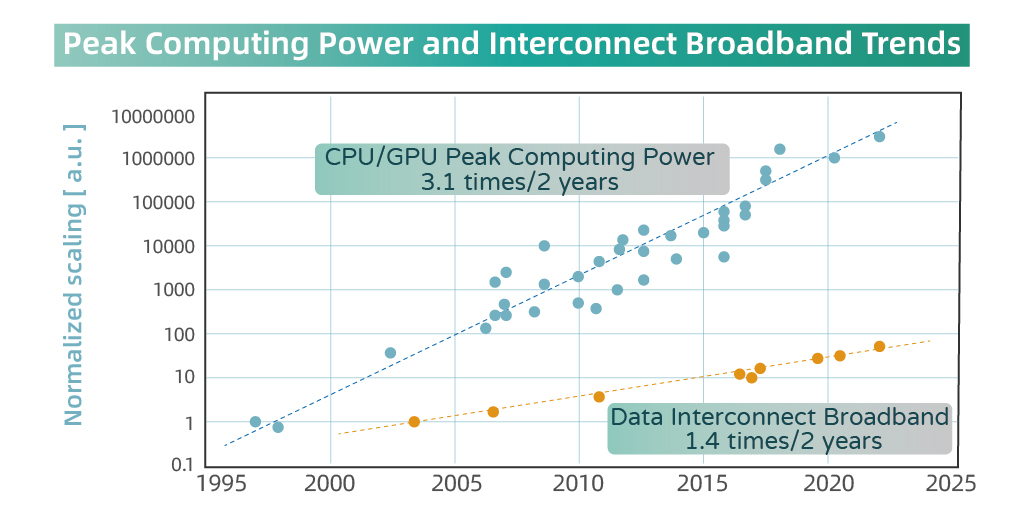
Figure 1 – Peak Computing Power and Interconnect Broadband Trends
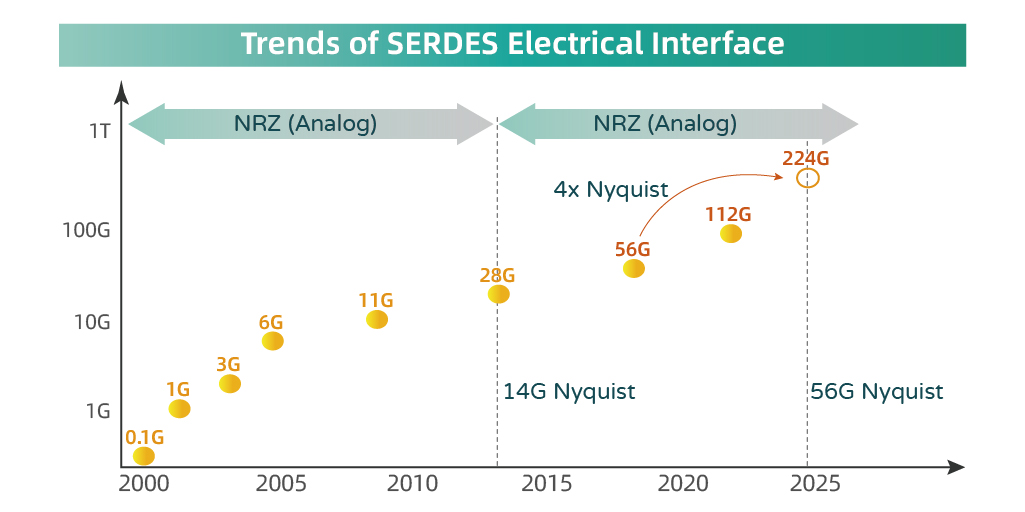
Figure 2 – Trends of SERDES electrical interface
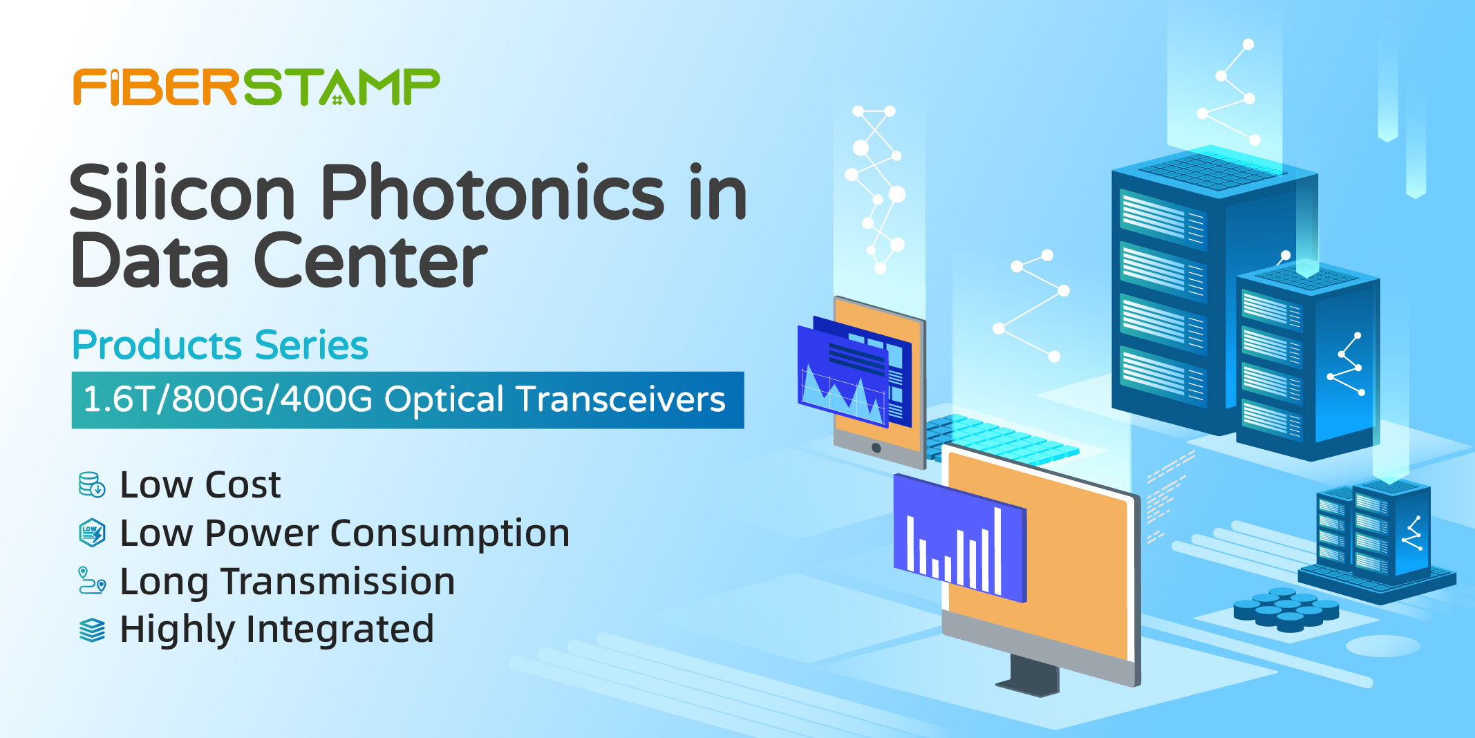
Silicon photonic data centers are mainly based on silicon optical data center switches and silicon optical transceivers.
Compared with other technologies, silicon optical chips have the following advantages: good performance of signal integrity SI transmission, high reliability, excellent performance of optical waveguide transmission, high integration, low cost, long-term technological evolution and etc.
1.Good Transmission Performance, High Reliability, Low Power Operation
The modulation mode of silicon optical technology module determines its better ability to overcome SI signal fading. The 100G PAM4 signal transmits high-speed electrical signals based on PCB (Printed Circuit Board), which is a great challenge for SI, and silicon light can better overcome on-board noise because of its modulation method, and can tolerate higher operating temperatures because of its temperature insensitive characteristics. Based on silicon optical platform and linear direct drive mode such as LPO/TRO/CPO, the system power consumption can be greatly reduced. This also reduces the total input cost. CPO (co-package optic) is a new unpluggable optical technology route to on-chip integrated package, which is highly challenging, but it can improve the total bandwidth capacity of exchange and transmission under the premise of the same space size. Because its main technical policy is to keep the photoelectric chip close, it can greatly reduce the energy demand and signal loss. At the same time, the volume of the switch and server is also reduced, and the space saved can further carry out heat dissipation treatment such as liquid cooling of the optical module, thus further reducing power consumption. At present, there are samples of 1.6T pluggable optical transceivers, and it is difficult to pluggable in terms of power consumption, crosstalk and optical modulator size with 3.2T. It is believed in optical industry that 1.6Tbps is the watershed of CPO and pluggable optical modules, and CPO technology and products are ready to be developed.
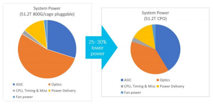
Figure 3 – 51.2T system power reduction from pluggable to CPO
Cisco: Thanks to CPO I/O innovations, product power consumption can be reduced by up to 50%, resulting in a total fixed system power reduction of up to 25% to 30%.
2.Good Waveguide Characteristics, High Integration and Low Cost Advantages
Silicon is transparent to the 1.1-1.6μm communication band, has excellent waveguide transmission characteristics, and high refractive index can form a large refractive index difference. Silicon photonics technology has higher integration and more embedded functions, which can improve the integration of the chip. The computing power center is generally parallel computation, which requires higher baud rate and more channels. Silicon photonic chips have the advantage of large-scale multi-channel integration, which greatly improves the feasibility of silicon optical technology to the next generation of technologies such as optical I/O. This is unmatched by wearing traditional techniques. Because the manufacturing process of silicon optical chips does not require a low-nanometer process, the cost of large-scale production is objectively reduced.
Figure 4 – Silicon photonic chips
In March 2024, Marvell showed the industry’s first 3.2Tb/s silicon optical CPO core product prototype, based on silicon optical and 3D photoelectric hybrid packaging technology, to achieve 32×200Gb/s photoelectric chip performance for AI cluster and cloud data center network switch interconnection.
3.Long-term Technology Evolution
The AI computing power center needs a greater computing power breakthrough, and the GPU computing power cluster is formed through networking, and the computing power cluster needs more optical interconnection components. AI network puts forward higher requirements for optical modules: higher bandwidth, low power consumption and high reliability of the product, high performance and low error code to meet the requirements of lossless network, improve KP-FEC margin, reduce KP-FEC error correction time, and achieve low latency.
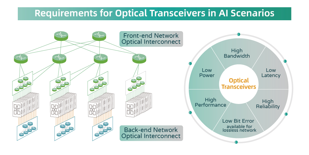
Figure 5 – Requirements for optical transceivers in AI scenarios
In the future generation of 1.6T networks, silicon photonics technology shows strong toughness, and only silicon photonics technology can complete the evolution from pluggable optical modules to next-generation networks. A relatively advanced NPO (Near-packaged optics) /CPO (Co-packaged optics) ecology based on silicon photonics has begun to take shape. In the future, CPO technology will become the mainstream business scheme. In OFC 2024, industry leader MARVELL demonstrated TRO DSP technology, and Broadcom showed Bailly, the industry’s first 51.2Tbps CPO silicon optical Ethernet switch with a single optical engine speed of 6.4T. In addition, we also see that many on-chip optical interconnection technologies represented by CPO are expanding to a wider range of optical I/O, and the future is expected to achieve GPU-to-GPU interconnection within the server and expand new application scenarios of optical interconnection.
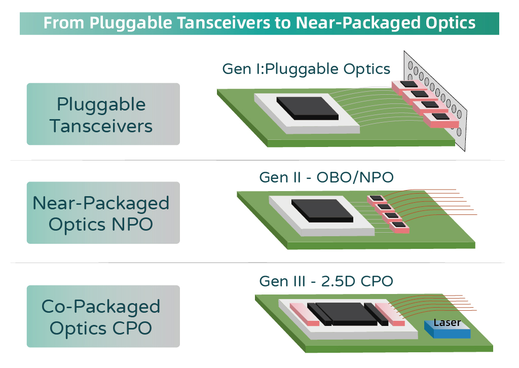
Figure 6 – Optical transceivers package evolution